| |
|
|
| Instruments in Lab |
| |
|
|
 |
|
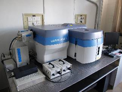
HORIBA Jobin Yvon ARAMIS Raman
Spectrometer
Automatic stage for XYZ Raman and PL mapping
Lasers: 532, 633, 785 nm
Detectors: CCD(200-1100nm); multi-channel InGaAs (800-1650nm)
Edge filter cutoff: 100 cm-1
|
| |
|
|
 |
|
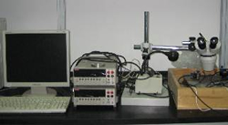
Fluorescence Microscope |
| |
|
|
 |
|
Keithley 2400 Source Meters |
| |
|
|
 |
|
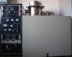
Multi-functional Coating Machine |
| |
|
|
 |
|
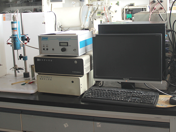
Electrochemical Workstation |
| |
|
|
 |
|
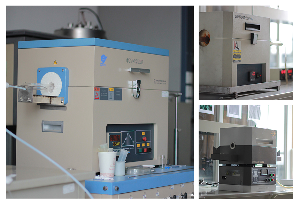
Thermo Tubular Furnace |
| |
|
|
 |
|
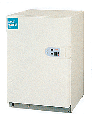
Sanyo MCO 15AC Incubator |
| |
|
|
 |
|
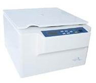
Centrifuge |
| |
|
|
 |
|
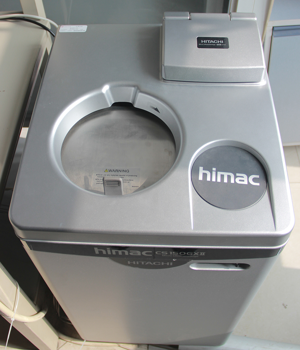
Hitachi Centrifuge |
| |
|
|
 |
|
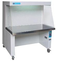
Clean Table |
| |
|
|
 |
|
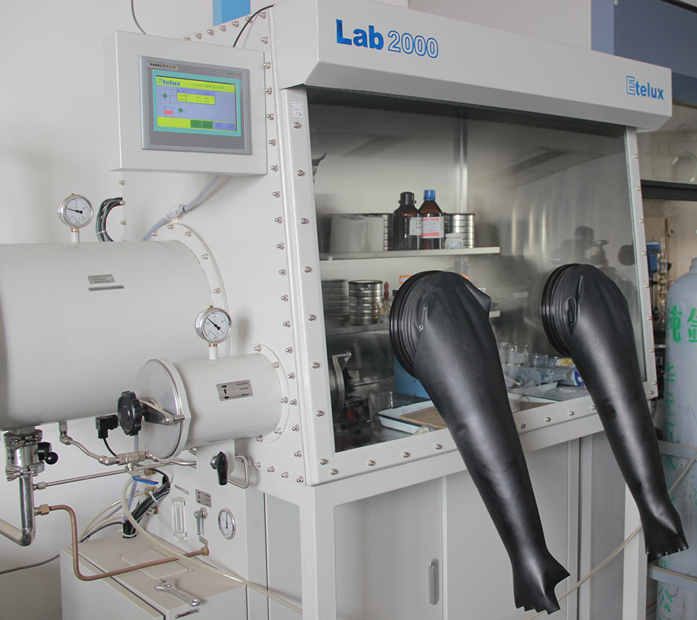
Glovebox |
| |
|
|
 |
|
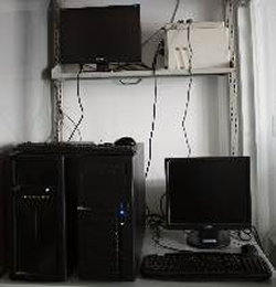
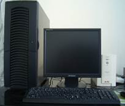
Server A for QC Calculation
Intel Xeon 5550 Quad Core CPU ×4, 16G ECC REG Memory,1.5TB Hardisk,Quadro NVS290 Graphic Card,APC 600W UPS
Server B for QC Calculation
Intel Xeon 5472 Quad Core CPU ×2, 16G ECC REG Memory,1.5TB Hardisk,Quadro NVS290 Graphic Card,APC 600W UPS |
| |
|
|
 |
|
Web Server and File Server
AMD Opteron270 Dual Core CPU ×2,4G ECC REG Memory,1TB Hardisk,APC 600W UPS |
| |
|
|
 |
|
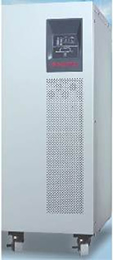
Santak UPS |
| |
|
|
| |
|
|
| Public Instruments (served
as Administrator) |
| |
|
|
 |
|
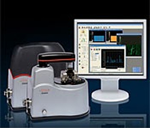
HORIBA NanoLog Fluorescence
Spectrometer
|
| |
|
|
 |
|
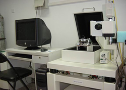
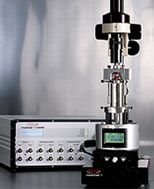
SII SPA400 SPM
Controller: SPI3800N
Scan Area: 100µm×100µm×2µm
Primary Imaging Mode: Tapping/Contact Mode in both Air and Fluid
Secondary Imaging Mode:EFM,KFM,MFM,Force Curve |
| |
|
|
 |
|
Veeco DiMultiMode V SPM(Peking University Nano-Fabration Lab)
Controller: Nanoscope V
Scanner: AS-12 (“E”) 10µm×10µm×2.5µm,AS-130 (“J”) 125µm×125µm×5.0µm
Software: Nanoscope V7.3
Primary Imaging Mode: Tapping/Contact Mode in both Air and Fluid,TRmode,STM
Secondary Imaging Mode: EFM,SEPM,MFM,LFM,Force Modulation,Phase Imaging,Force Curve,Force Volume
Application Module: TUNA2,SCM
|
| |
|
|
 |
|
Veeco DiInnova SPM(Peking University Nano-Fabration Lab)
Controller: NanoDrive
Scanner: Small Area Scanner 10µm×10µm×2.5µm,Large Area Closed-Loop Scanner 100µm×100µm×7.5µm
Software: SPMLab v7.11
Primary Imaging Mode: Tapping/Contact Mode in both Air and Fluid, STM
Secondary Imaging Mode: EFM,MFM,LFM,Phase Imaging,Force Curve,Nanoplot
Closed-Loop Control |
| |
|
|