

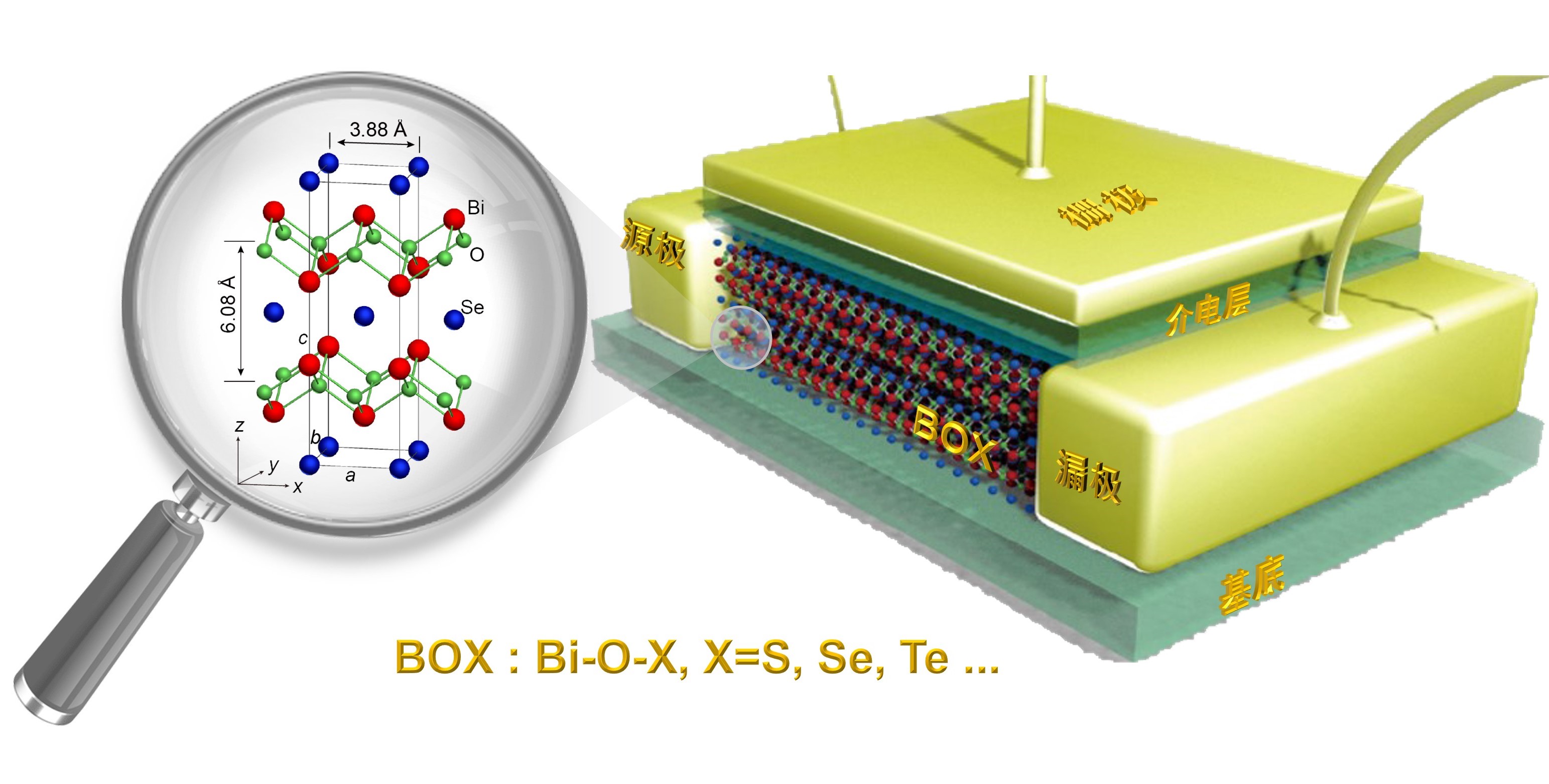
2D semiconducting Bi2O2Se with ultrahigh mobility
The Peng research group realized the controlled syntheses of high-mobility semiconducting 2D crystals--- layered bismuth oxychalcogenides (BOX, Bi2O2X: X = S, Se, Te), and are vigorously exploring their vistas in electronics and optoelectronics. (Jinxiong Wu, et al. High electron mobility and quantum oscillations in non-encapsulated ultrathin semiconducting Bi2O2Se. Nature Nanotechnology 2017, 12, 530
https://www.nature.com/articles/nnano.2017.43

超平整氮化硼单晶晶圆的可控制备与高介电金属栅集成
Based on ultra-flat boron nitride single crystal wafers, Peng research team designed and prepared a transportable ultra-flat boron nitride/hafnium oxide/metal composite gate electrode, achieving high-quality van der Waals integration of the composite gate electrode with 2D materials such as graphene, and showing excellent grid control performance. Specifically, the research team used the semiconductor process-compatible atomic Layer deposition technique (ALD) to prepare ultra-thin, dense and uniform films of high dielectric hafnium oxide on ultra-flat single crystal boron nitride /Cu0.8Ni0.2/ sapphire wafers and deposited the top electrode. A transferable, high-quality super-flat boron nitride/hafnium oxide/metal composite gate electrodeis obtained. The equivalent oxide layer thickness of the prepared composite gate medium can reach 0.52 nm, meeting the requirements of the international device and system roadmap 2025, and the leakage current (2.36×10⁻⁶ A cm−2) meets the requirements of transistor low power consumption.
Nature Mater. 2024, 23, 1495. Highlighted by Nat. Mater News & Views

隐藏自旋极化诱导的偶数量子霍尔效应
Recently, the research team's experiments found that a new even quantum Hall effect (filling factor ν = 2, 4, 6, 8...) appears in high quality layered bismuth selenide under a pulsed strong magnetic field of 50 T. , while odd-numbered quantum Hall platforms (fill factors ν = 1, 3, 5, 7...) All missing. It is found that the new even quantum Hall effect under strong magnetic field in bismuth selenide is due to its unique hidden spin polarization effect. In the [Bi2O2]2+ conductive channel of layered bismuth selenooxide, the upper and lower bismuth atomic layers have great spin polarization due to symmetry breaking, but the spin polarization of the two layers of bismuth atoms is exactly opposite, and the special structure of double-layer Rashba is formed in [Bi2O2]2+Peng group firstly discovered and regulated the unique even quantum Hall effect in bismuth selenide. The results show that bismuth selenooxide, a two-dimensional semiconductor with strong spin-orbit coupling effect and ultra-high mobility, is an ideal material platform for discovering novel quantum Hall effect, regulating band topology and spin texture, exploring spin-related physical phenomena, and constructing high-speed and low-power spintronics devices.
Nature Nanotech. 2024, 19, 1452
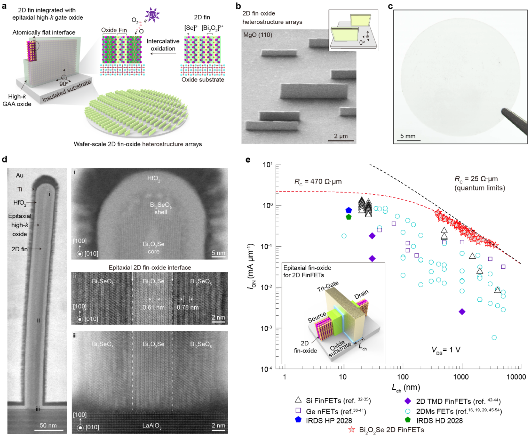
首例外延栅介质集成型二维鳍式晶体管
The Peng group achieved the wafer-scale synthesis of 2D semiconductor fin/high-k gate oxide heterostructure array, and fabricated the high-performance 2D FinFET, which was pubuliched on Nature entitled as "2D fin field-effect transistors integrated with epitaxial high-κ gate oxide" . The as-fabricated 2D fin/oxide heterostructure has ultra-flat interface and ultra-thin fin thickness down to 1unit cell (1.2 nm), which was compatible to wafer-scale high-density and site-specific synthesis. The as-fabricated 2D fin field-effect transistors (FinFETs) based on Bi2O2Se/Bi2SeO5 epitaxial heterostructures exhibit high electron mobility (μ) up to 270 cm2 V-1 s-1, ultra-low off-state current (IOFF) down to ~1 pA μm-1, high on/off current ratios (ION/IOFF) up to 108, and high on-state current (ION) up to 830 μA μm-1 at 400-nm channel length, which meet the low-power specifications projected by the International Roadmap for Devices and Systems (IRDS). The 2D fin-oxide epitaxial heterostructures open up new avenues for the further extension of the Moore's law.
Nature 2023, 616, 66.

自组装超结构电镜载网抑制冷冻制样中的气液界面效应
Based on the self-assembly behavior of stearic acid molecules on the graphene surface, the research team obtained a large area of self-supporting graphene films on the liquid surface, namely GSAMs, and the graphene electron microscope carrier mesh produced can effectively inhibit the gas-liquid interface effect in the cryo-electron microscope sample preparation. The method is simple and easy to use, and avoids the pollution caused by the traditional assisted transfer of polymers. At the same time, the research team compared GSAMs with surfactants commonly used in cryoelectron microscopy imaging, and found that GSAMs can better improve the concentration and orientation of protein molecules in the ice layer, which is conducive to efficient and high-resolution three-dimensional reconstruction. Combining the above advantages, the research team used GSAMs carrier nets to perform high-resolution structural analysis of a variety of proteins at different scales. Including streptavidin (52 kDa) at 2.6A resolution, human angiotensin-converting enzyme 2-novel coronavirus spike protein receptor-binding domain complex (ACE2-RBD) at 3.3A resolution, 100 kDa) and 2.0A resolution of the 20S proteasome (690 kDa).
Nature Commun. 2024, 15, 7300.
Nature Methods 2023, 20, 123.

集成型多通道二维鳍式晶体管
The excellent electrical properties of high κB self-oxide Bi2SeO5 integrated multi-channel 2D fin transistors demonstrate that 2D Bi2O2Se fin arrays can work together and have the potential to realize complex logic operations through multi-fin integration. In the future, with the further optimization of step fabrication methods and the precise control of step spacing, the regularly arranged high-density two-dimensional Bi2O2Se fin arrays are expected to provide the material basis for the large-area integration of two-dimensional fin transistors (2D FinFET) and two-dimensional vertical enclosing gate devices (2D VGAA). It is of great significance in the future development of micro-nano electronic devices with high computing power and low power consumption.
Nature Commun. 2024, 15, 3622.

石墨烯高响应度光通信探测器
This study is the first to achieve the fabrication of torsified bilevel graphene and silicon waveguide integrated photodetectors, combined with tBLG's unique vHs band structure and device structure design, showing excellent performance with high responsiveness of 0.65A/W and 3dB bandwidth of 65GHz (limited to measurement equipment). In addition, through the preparation of large-area tBLG device arrays, and the verification of high responsiveness (0.46±0.07A/W) and high width (36±2GHz), the excellent potential of tBLG with vHs and linear dispersion band structure and silicon optical heterosynthesis for large-scale high-performance optical communication devices is proved. In particular, considering the development of tBLG wafer level growth and graphene wafer level transfer technology with controlled torsion Angle.
Nature Commun. 2024, 15, 3688.

Roll-to-roll CVD mass production of graphene film
The Peng research group has achieved the mass production of graphene film via continuous roll-to-roll chemical vapor deposition and non-destructive lamination transfer process .
Nano. Lett. 2015, 4206–4213;
Advanced Materials 2015, 27(35), 5210;
Advanced Materials 2015, 30, 1800996.
https://onlinelibrary.wiley.com/doi/10.1002/adma.201502560
https://pubs.acs.org/doi/10.1021/acs.nanolett.5b01531
https://onlinelibrary.wiley.com/doi/10.1002/adma.201800996